Center for Solar Energy Research and Applications (ODTÜ-GÜNAM)
TA76 – IMEC-UNIAnkara-ODTÜ-GÜNAM
Location
Üniversiteler Mah. Dumlupınar Bul. No:1, Çankaya
6800 Ankara, Turkey
Description
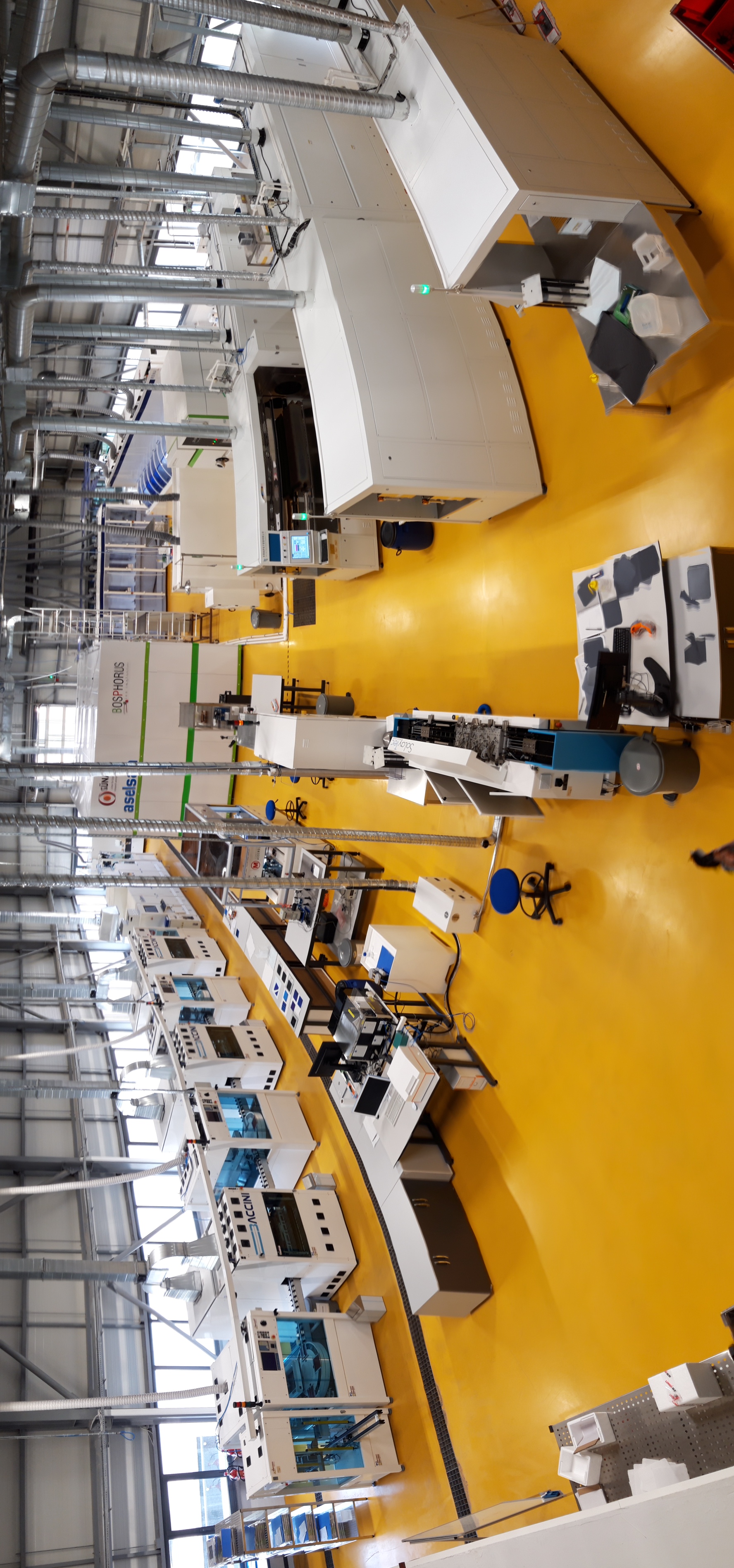
ODTÜ-GÜNAM pilot scale Photovoltaic (PV) production facility (GPVL), which has a 600 m2 production area with ≈200 wafers/h manufacturing capacity, is mainly capable of producing PERC/TOPCon/IBC type full size (M2/G1) silicon solar cells. Although the pilot line is designed for continuous cell production, it has the flexibility to provide local service at each production step.
Services offered include the production of half-finished cells for material and process testing and testing and applying new materials for solar cell production or other Si wafer-based studies. Almost all chemical processes used in Si-based solar cell fabrication, such as saw damage etching, texturing, single-side etching, surface polishing, etc., can be carried out with industrial devices in the PV pilot line. Single-side or symmetrical phosphorus (P) and boron (B) doping to form homogeneous or localised emitters, silicon dioxide (SiO2) layer growth and low- and high-temperature annealing can be performed on M2/G1 sized silicon wafers. Additionally, phosphorus (P) and boron (B) can be implanted on Si wafers.
Deposition processes served include silicon nitride (SixNy) and silicon oxynitride (SiOxNy) deposition by PECVD, alumina (Al2O3) coating by ALD, and polysilicon deposition by LPCVD. Laser processes include scribing/cutting, dielectric layer ablation, local laser doping, and surface structuring. Metallisation services such as screen printing, metal evaporation, or plating are also offered in the PV production line.
All processes described above are offered to external users. All proposed processes will be carried out under the supervision of expert researchers or engineers from ODTÜ-GÜNAM. Should you need any detailed information about the services described above that you are interested in benefitting from, please do not hesitate to get in touch.
Testing Capabilities
Wet chemical processes for silicon-based solar cell production, thermal diffusion and ion implantation, surface passivation and anti-reflective layer (ARC) deposition, laser processes, solar cell metallisation.
Technical Equipment
- Texturing & Cleaning Equipment (RENA BatchTex)
The system is fully automated and capable of sequential chemical processing on silicon wafers arranged in cassettes of 50 wafers (M2/G1) capacity. The production speed in the system can reach over 1000 wafers per hour.
- Single Sided Etching Equipment (RENA InPilot)
The system is an in-line industrial tool for single-sided etching (Si, Poly-Si, PSG, BSG) on silicon wafers.
- Diffusion Furnaces (Phosphorus (P) and Boron (B))
Doping furnaces can accommodate up to 270 wafers per run, with operating temperatures reaching up to 900°C for Phosphorus doping and 1000°C for Boron doping. BBr3 is the precursor for boron doping, while POCl3 is employed for phosphorus doping.
- Ion Implanter (Phosphorus (P) and Boron (B))
Ion implanter is capable of implanting both phosphorus and boron ions, which are essential for creating p-type and n-type regions in silicon-based solar cells. The implanter operates within 5 to 40 keV energy ranges. One of the significant advantages of our implanter is its capability for both full-area (M2/G1) and localised doping.
- Atomic layer Deposition (ALD) Equipment (SALD, SoLayTec)
Spatial Atomic Layer Deposition (sALD) is a technique for depositing thin films layer by layer on substrates in a controlled manner. Using the TMAI precursor, it is possible to deposit highly uniform Alumina (Al2O3) layers as a passivation layer, especially for photovoltaic applications.
- Low-Pressure Chemical Vapor Deposition (LPCVD) (Poly-Si, SiO2)
- Plasma-enhanced chemical vapor deposition (PECVD) (SiNx, SiNxOy)
- Laser Equipment (Innolas Solutions GmbH)
The picosecond laser system allows processing at both 532nm and 1064 nm wavelengths. Scribing/cutting, dielectric layer ablation, local laser doping, and surface structuring are the processes offered.
- Screen Printer Line (Ag, Al)
The Baccini rotary screen printer is a highly efficient and versatile tool widely used in the metallisation process of solar cells. Renowned for its precision and reliability, the Baccini rotary screen printer enables the deposition of fine metal contacts on the surface of solar cells, which is a critical step in enhancing their electrical performance.
- Fast Firing Furnace
- Electron beam Deposition Equipment (Au, Ag, Al, Cu)
The electron beam (e-beam) deposition system is a versatile and powerful tool used in solar cell metallisation and the deposition of various layers, such as electron transport layers (ETL) or hole transport layers (HTL). This advanced technique employs a focused beam of high-energy electrons to evaporate materials, which then condense to form thin, uniform films on the substrate.
The e-beam deposition system at ODTÜ-GÜNAM is compatible with a wide range of materials, including aluminium (Al), gold (Au), copper (Cu), and molybdenum (Mo), among others.
- Plating Equipments (Nb Technologies, RENA) (Ni, Cu, Ag)
Metallisation by plating refers to the process of electrochemically depositing metal ions from a liquid electrolyte onto a mostly conductive surface. ODTÜ-GÜNAM research infrastructure offers a plating metallisation process with all three methods, namely electroplating, light-induced plating (LIP) and bias assisted plating (BIP).
Additional information
Technology Readiness Level: 4-6
Special considerations: N/A
Technology clusters: PV
Website: https://odtugunam.org
Availability: All year
Provision of tools to prepare data sets in a FAIR way: Yes